PHASIS is involved in several applied research projects with both academic and industrial partners. The flexibility of PHASIS' equipment allows the production of thin films with tailored properties.
Surface quality control is a pertual challenge. PHASIS provides local probe surface analysis using Atomic Force Microscopy (AFM) and/or Scanning Tunneling Microscopy (STM).
PHASIS is therefore open to any special request.
-
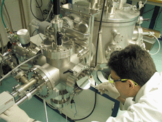
Thin film laboratory at PHASIS
-
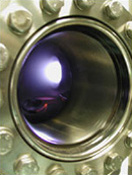
Close-up inside the system
during thin film growth -
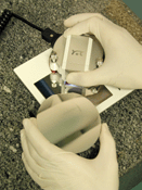
Wafer nanoscale surface analysis - Atomic Force Microscopy